Four bit adder or subtractor using 7483 Logic diagram of ic 7483 draw a neat circuit of bcd a Adder bit ic 7483 using binary full parallel adders four explain ques10
Circuit Diagram For 4 Bit Binary Adder Using Ic 7483 Wiring Digital
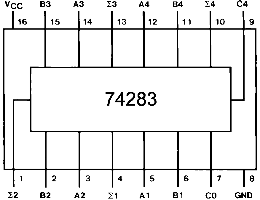
Ic 7483 pin diagram circuit Circuit image 74ls83 4-bit binary full adder ic with fast carry
Design and implementation of 10’s complement circuit using ic-7483
Ic 7483 internal circuit diagramDesign and explain 8 bit binary adder using ic 7483. 9+ 7475 pin diagramImplement 10 bit comparator using ic 7485..
Design and implementation of 10’s complement circuit using ic-7483Circuit diagram for 4 bit binary adder using ic 7483 Design and implementation of 10’s complement circuit using ic-7483Bcd adder truth table.
Using ic 7485 design an 8 bit comparator
Circuit diagram for 4 bit binary adder using ic 74837485 ic 4-bit magnitude comparator [diagram] logic diagram of ic 7483Ic 7483 pin diagram circuit.
74hc83 full adder ic pinout, datasheet, equivalent working, 50% offCircuit diagram for 4 bit binary adder using ic 7483 The counting thread74ls83 pinout.

Circuit diagram for 4 bit binary adder using ic 7483
Pinout adder datasheet carryCircuit diagram for 4 bit binary adder using ic 7483 Circuit diagram for 4 bit binary adder using ic 7483Circuit diagram for 4 bit binary adder using ic 7483.
Design and implementation of 10’s complement circuit using ic-74837485 ic bit comparator using diagram cascade pins any logic compare shown words below 7483 4-bit binary full adderDesign and explain 8 bit binary adder using ic 7483..

Circuit diagram for 4 bit binary adder using ic 7483 wiring core
Ic 7483 pin configuration7485 ic comparator bit magnitude datasheet Ic adder 7483 bit binary full using pooja joshi parallel descriptionCircuit diagram for 4 bit binary adder using ic 7483 wiring digital.
.


9+ 7475 pin diagram - NajmaCallahan

Bcd Adder Truth Table

Circuit Diagram For 4 Bit Binary Adder Using Ic 7483 Wiring Digital

Design and Implementation of 10’s Complement Circuit Using IC-7483

Design and Implementation of 10’s Complement Circuit Using IC-7483

Logic Diagram Of Ic 7483 Draw A Neat Circuit Of Bcd A - vrogue.co

Ic 7483 Pin Diagram Circuit

Circuit Diagram For 4 Bit Binary Adder Using Ic 7483 Wiring Core - Vrogue
